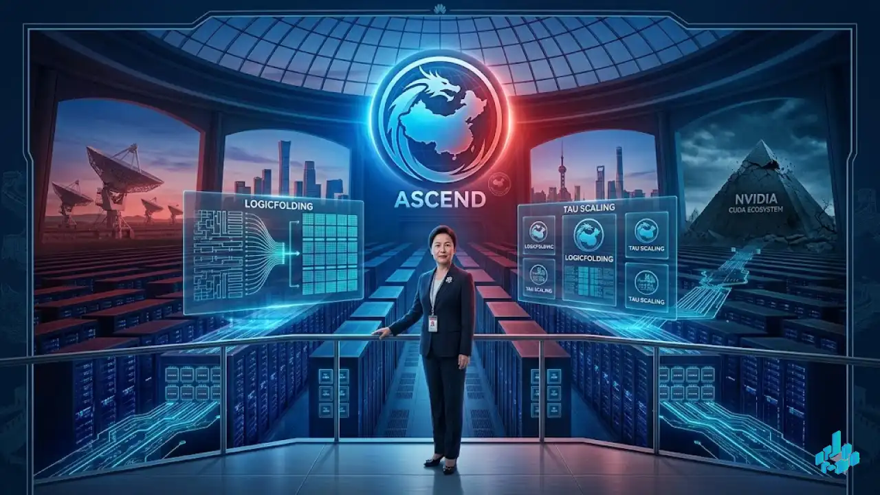
Instead of copying Western lithographic methods banned by sanctions, Chinese engineers proposed a fundamentally new mathematical and physical approach to transistor layout. A clear track has been declared: achieving element density of the 1.4nm level by 2031. This approach is already being successfully implemented in the new Ascend AI chip family. Heading the operations is the legendary He Tingbo, who has earned the status of "chip queen" in the press.
Simultaneously, Huawei presented a complete full-stack solution for AI data center infrastructure. The PRC is officially building a fully independent ecosystem, replacing American accelerators (NVIDIA Blackwell) and software (CUDA) with sovereign hardware and their own LEM models. The effect of the sanctions proved to be the opposite: China has created a closed AI loop immune to external pressure.
Source: Huawei / Reuters / Data Center Dynamics
HardwareHuaweiTau ScalingChinaAscend