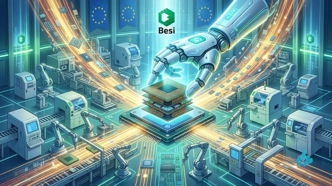
The key driver is hybrid bonding technology. When manufacturing modern AI accelerators and HBM memory stacks, classic soldering is no longer capable of providing the required contact density and heat dissipation. Hybrid bonding allows silicon dies to be joined directly at the atomic level. Without Besi equipment, the production of next-generation chips for data centers is simply blocked. This report proves that investors seeking defensive assets during the AI boom are finding them in the utilitarian industrial engineering segment.
Source: Besi / Reuters
HardwareBesiSemiconductorsHybrid BondingDeepTech