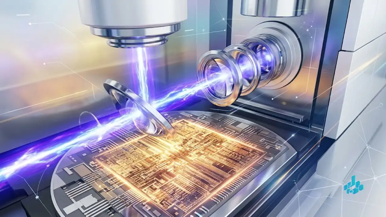
This announcement means the sub-2-nanometer process barrier has been physically overcome. High-NA EUV equipment allows the printing of transistors with phenomenal density, which is critical for the next generation of AI accelerators and CPUs. Without these machines, which cost hundreds of millions of dollars each, the progression of architectures (like those developed by NVIDIA or Apple) would halt due to the thermal and physical limitations of silicon. The transition to High-NA EUV marks the beginning of a new, historically most expensive cycle of semiconductor factory modernization.
Source: ASML / Intel / Reuters
DeepTechASMLHigh-NA EUVHardwareSemiconductors